

The Blackwell architecture is considered a successor to the widely popular NVIDIA Hopper Architecture. The NVIDIA H100 and NVIDIA H200 are some of the popular GPUs that belong to the Hopper family.
The NVIDIA Blackwell architecture is a major advancement when compared to its predecessor in areas such as GPU design, accelerated computing, high-performance graphics, and more. The architecture is ideal for high-end AI workloads, deep-learning tasks, 3D-rendering, and data analytics since it provides the perfect balance of power and performance!
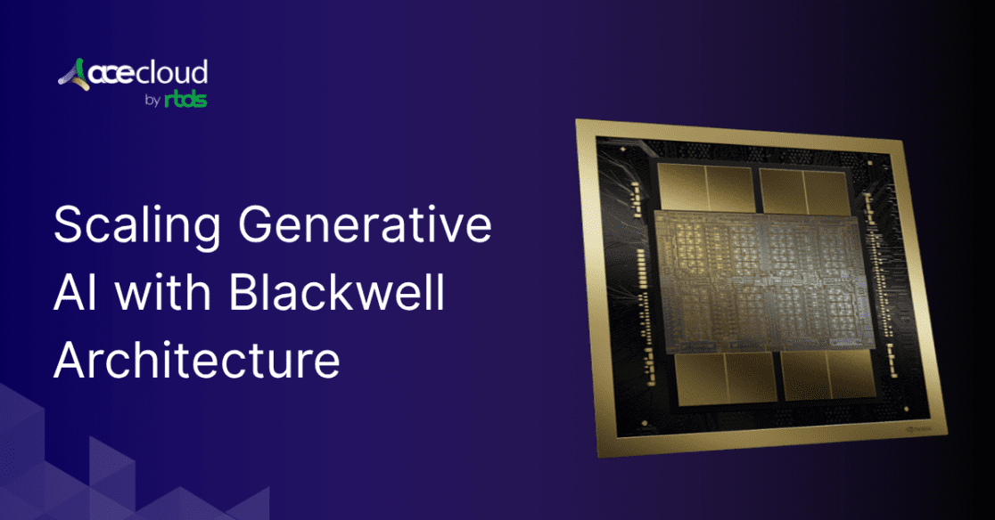
The GPUs based on the Blackwell architecture pack 208 billion transistors and are manufactured using a custom-built TSMC 4NP process. Dual-die design, fifth-generation tTensor cores, confidential computing with TEE-I/O, and 25x lower cost & energy consumption for real-time inference as comparison to Hopper are some of the highlights of the Blackwell architecture.
In this blog, we look at how the Blackwell architecture is laying out the foundation of the future of Generative AI.
What is Blackwell Architecture
The Blackwell architecture by NVIDIA, introduced in March 2024, is named after the mathematician David Harold Blackwell. It is the successor to the popular Hopper architecture. The Blackwell architecture packs a lot of powerful features that are expected to accelerate AI, machine learning, and HPC (High-Performance Computing) workloads.
Blackwell GPUs – B100, B200, and GB200, can also handle traditional HPC-like simulations, scientific computing, weather modeling and more. Over & above, it can also cater to seamless handling of AI-driven HPC workloads like AI-accelerated simulations, and physics-informed neural networks.
The Blackwell GPU architecture ushers in a new era of computing, enabling organizations to build and run real-time Generative-AI on trillion-parameter Large Language Models. That’s not it, all of this can be achieved with 25x less cost and energy consumption than the Hopper architecture.
Shown below are the workstations/GPUs/accelerators based on the Blackwell architecture:
| Product | Segment | Specifications |
|---|---|---|
| RTX PRO 6000 Blackwell | Workstation | 188 SMs 2.85 GHz maximum clock speed 96 GB GDDR7 750mm2 die size 5th-gen Tensor Cores 4th-gen RT Cores |
| GeForce RTX 5090 | Consumer GPU | 21,760 CUDA cores 2.41 GHz maximum clock speed 32 GB GDDR7, 512-bit memory interface 5th-generation Tensor Cores 4th-generation RT Cores |
| GeForce RTX 5080 | Consumer GPU | 10,752 CUDA cores 2.62 GHz maximum clock speed 16 GB GDDR7, 256-bit memory interface 5th-generation Tensor Cores 4th-generation RT Cores |
| RTX PRO 4000 Blackwell SFF | Workstation GPU | 8,960 CUDA cores 24 GB GDDR7 (ECC) memory ~432 GB/s memory bandwidth 5th-generation Tensor Cores 4th-generation RT Cores Small-form-factor, dual-slot active form-factor |
| RTX PRO 2000 Blackwell | Workstation GPU | 4,352 CUDA cores 16 GB GDDR7 (ECC) memory ~288 GB/s memory bandwidth 5th-generation Tensor Cores 4th-generation RT Cores ~545 AI TOPS |
| Blackwell Accelerators: GB200, B200, B100 | Data-center superchip / Rack-scale / Data-center accelerators | High-bandwidth HBM3e (multi-TB capacity at rack/system scale) NVLink 5 & NVSwitch for multi-GPU scaling; integrates tightly with Grace CPUs (GB200) Built on 5th-gen Tensor Cores (for AI) and optimized SM design |
Data processing, engineering simulation, EDA, Computer-Aided drug design, quantum computing, and generative AI are some of the transformative industries that would benefit significantly by adopting the NVIDIA Blackwell GPU architecture.
Features of Blackwell Architecture
AI-driven applications require immense computational power which cannot be met with CPUs. This is where GPUs, particularly GPUs based on the Blackwell architecture can have a significant impact on performance, power and throughput! For businesses weighing CPU vs. GPU, NVIDIA’s Blackwell GPUs stands-out owing to power and efficiency gains for AI and data-intensive workloads.
Here is the six-fold set of breakthrough technologies that are instrumental in enabling Blackwell GPUs to realize training and real-time LLM inference for models that can scale up to 10 trillion parameters.
Powerful Multi-Die (or Multi-Chip) GPU
Prior to the Blackwell architecture, the GPUs from NVIDIA always employed a monolithic (or single-die) GPU design. Here, a single silicon die contains all the essential components such as the Streaming Multiprocessors (SMs), cache, memory controllers, and graphics engines.
Scaling in single-die GPUs becomes limited due to yield reductions, limited coherent memory sharing between GPUs, and power/thermal constraints at larger die sizes. The Multi-Chip Module (MCM) design overcomes these limitations with the multi-die GPU architecture.
NVIDIA Blackwell-architecture GPUs with a multi-die design pack 208 billion transistors in total. The GPU is manufactured using a custom-built TSMC 4NP process. Every Blackwell-based GPU features two reticle-limited dies, each containing 104 billion transistors. The dies are linked by a 10 TB/s chip-to-chip interface to function, thereby creating a unified GPU.
To be more precise, Blackwell combines two GB100 GPU dies that are interconnected through NVIDIA’s NV-High Bandwidth Interface (NV-HBI). All of this helps in providing ultra-high inter-die communication bandwidth, reduced latency, seamless cache coherency, and unified memory access across the GPU dies.
The MCM design in the Blackwell architecture enables better scaling of AI workloads, with lower power consumption and much higher-bandwidth efficiency in comparison to single-die GPUs.
Second-Generation Transformer Engine (FP4 Precision)
For starters, a Transformer Engine (TE) is a library for accelerating transformer models on NVIDIA GPUs that include the usage of 8-bit floating point (FP8) precision on Hopper, Ada, and Blackwell GPUs. There is a heavy reliance on computationally intensive attention mechanisms and matrix multiplications, both of which demand significant processing power and memory bandwidth.
The transformer engine provides better performance with lower memory utilization in both training and inference. The transformer engine was first introduced in the Hopper architecture-based H100 GPU. Transformer-based neural network architectures like GPT and BERT relied heavily on the transformer engine, as it was instrumental in optimizations primarily through mixed-precision support (e.g., FP16 and FP8).
The transformer engine in the Hopper architecture performed well in self-attention and accelerating matrix multiplications but it faltered with extremely large models. This is primarily due to higher memory bandwidth usage and bottlenecks related to the precision. All these shortcomings are overcome by the second-generation transformer engine (TE 2.0) in the Blackwell architecture.

Figure 1: Comparison between Blackwell and Hopper (Source: NVIDIA)
Transformer Engine 2.0 supports native hardware acceleration for new micro-scaling data formats such as 4-bit floating point (FP4) and FP6. Lower-precision formats (i.e., FP4 and FP6) help in significant reduction of memory bandwidth demands, along with enhancement of computational throughput. This enables accelerated LLM training, inference and deployment of transformer models that effortlessly scale up to 10 trillion parameters.
The custom NVIDIA Blackwell Tensor Core technology combined with NVIDIA TensorRT-LLM and NeMo Framework innovations help in accelerating inference and training for LLMs and Mixture-of-Experts (MoE) models. NVIDIA Blackwell Ultra Tensor Cores also provide 2x faster attention-layer acceleration and 1.5x more AI compute FLOPS when compared to its predecessor – the Hopper architecture.
Secure AI & Confidential Computing
Confidential Computing in NVIDIA Blackwell has immensely strong hardware security that keeps the sensitive data protected all the time. Also, it protects the AI-models from any unauthorized access.
Blackwell is the first GPU that is equipped with the TEE-I/O support. TEE (Trusted Execution Environment) is a protected execution environment that ensures the confidentiality and integrity of code and data. With TEE-I/O, the TEE model is also extended to include the I/O (Input/Output) data movement path. With TEE-I/O, all the potential security risks are at bay, as data & I/O operations remain protected through end-to-end encryption.
Even with E2E encryption, there is no compromise on the throughput since Confidential Computing is capable of delivering nearly identical throughput performance when compared to the unencrypted modes! Support of native (or inline) protection over NVIDIA NVLink and unmatched performance makes Blackwell an ideal GPU for data-sensitive industries like healthcare and financial services.
Fifth-Generation NVLink and NVSwitch
Hopper family-based GPUs like H100 had the fourth-generation NVLink (i.e. NVLink 4.0) that could connect hosts and accelerated processors at rates up to 900 gigabytes per second (GB/s). Though it provided high speed GPU-to-GPU communication, it had scalability limitations in large-scale, distributed AI training and intensive HPC workloads. All these issues were resolved in NVLink 5.0.
The fifth-generation NVLink interconnect has the potential to deliver 1.8 TB/s of bidirectional bandwidth per GPU. It can be scaled up to 576 GPUs, thereby helping you achieve accelerated performance for trillion and multi-trillion-parameter AI models.
Over and above, NVSwitch (i.e., NVLink Switch chip) achieves an aggregate 130 TB/s GPU bandwidth within a single 72-GPU pod (NVL72). It also supports advanced in-network computing, Scalable Hierarchical Aggregation and Reduction Protocol (SHARP) for efficient scaling. Reduced data transfer latency, accelerated data transfers, inter-GPU synchronization enabled by NVLink and NVSwitch enables seamless memory sharing and cooperative processing across multiple GPUs.
Decompression Engine
Data analytics and database workflows have primarily relied on CPUs for compute. All of this is set to change with Blackwell GPU, as it has an on-die decompression engine that accelerates data loading and analytics.
It has the support for the latest compression formats such as LZ4, Snappy, and Deflate. This keeps the CPU free for taking up other tasks. This engine is also instrumental in speeding up end-to-end data pipelines such as databases, Spark analytics, and ETL.
Blackwell products integrate with NVIDIA Grace-class CPUs and NVLink-C2C interconnects; for example, Grace-linked systems expose very high interconnect bandwidth (NVIDIA documents 900 GB/s interconnect figures for certain Grace pairings). This helps improve performance and reduce costs for data science workloads.
Reliability, Availability, and Serviceability (RAS) Engine
The Blackwell architecture adds a layer of intelligent resiliency with a dedicated RAS engine. It realizes intelligent resiliency by diagnosing faults early and forecasting issues to minimize downtime.
The AI-powered predictive-management analytics keeps monitoring thousands of hardware/software data points. This preventative maintenance capability helps maximize uptime, improve efficiency, and save time, energy and computing costs!
What are the Primary use cases of NVIDIA Blackwell
As seen so far, the Blackwell architecture by NVIDIA combines powerful hardware advancements with equally impactful software features. With this, it is set to have a monumental impact on numerous industries and AI applications that demand superlative performance with improved energy efficiency.
Here are some of the major domains that are set to benefit from the Blackwell family of GPUs:
Generative AI and LLMs
Blackwell’s breakthrough features such as second-generation Transformer Engine (TE 2.0), advanced Tensor Cores, enhanced CUDA framework and decompression engine, make it an ideal GPU for handling massive generative AI models! Enterprises leveraging large-scale transformer-based language models such as GPT and BERT can significantly reduce training and inference times.
TensorRT, the deep learning inference optimizer and runtime,on NVIDIA’s Blackwell architecture plays a major role in real-time AI inference and efficient deployment at scale. TensorRT works in tandem with other blocks namely – 5th-generation Tensor Cores, TE 2.0, and NVLink & NVSwitch.
This entire combination accelerates real-time inference performance, while improving power efficiency and scalability across diverse AI workloads. High-throughput, low latency real-time applications like chatbots & GPT-based language assistants, autonomous driving, real-time video analytics, and edge AI would largely benefit from accelerated training & real-time inference of the Blackwell architecture.
AI Reasoning and Agentic AI
The advent of powerful Gen-AI models and high-performant GPU infrastructure has also resulted in the rise of the AI Agent Economy. AI Agents can reason, plan and coordinate multiple AI models & tools for performing complex tasks. You can also check out the AI Agents vs. LLMs blog that dives deep into the fine-line of differences between them.
Agentic systems rely on iterative prompting, planning and chaining of LLMs in loops for task refinement and multi-agent coordination. However, these approaches are not only compute-heavy but also token-intensive owing to repeated generation and analysis. The NVIDIA Blackwell architecture provides acceleration for AI workloads, optimizing data processing pipelines for Agentic AI.
The NVIDIA HGX B300 NVL16 GPU features 16 dual-Blackwell GPU package modules with up to 2.3 TB of HBM3e memory & high-speed NVLink interconnects offers 11x faster LLM inference and 7x AI compute for multi-step agentic simulations.
Along with Agentic AI, AI reasoning also demands orders of magnitude and more computing performance. The full-stack NVIDIA AI platform in the Blackwell product portfolio and NVIDIA Dynamo (open-source inference framework) massively scales up reasoning AI services while reducing response times and model-serving costs.
Graphics and AI-driven Visualization
GeForce RTX 5090, RTX 5080, RTX 5070 Ti, and RTX 5070 are the first NVIDIA GeForce graphics cards based on the new RTX Blackwell architecture. All four GPUs are designed to deliver exceptional performance in their GPU class and provide groundbreaking new AI features for gamers & creator/professional users.
AI Management Processor (AMP) – a dedicated RISC-V-based processor integrated into the Blackwell GPU, is a fully programmable context scheduler on the GPU designed to offload scheduling of GPU contexts from the system CPU. AMP enhances the scheduling of GPU contexts in Windows to more efficiently manage different workloads running on the GPU. The AMP enables efficient multitasking between graphics rendering and AI workloads.
DLSS 4.0 (Deep Learning Super Sampling 4.0) is NVIDIA’s latest suite of AI-driven neural rendering technologies that debuted with the RTX Blackwell architecture. DLSS 4 leverages advanced AI algorithms and fifth-generation Tensor Cores for delivering significant performance boosts, enhanced image quality, and reduced latency in real-time graphics applications.

Figure 2: DLSS 4 Multi Frame Generation
The AI multi-frame generation boosts DLSS 4’s frame rates up to 2x over the previous DLSS 3/3.5, while maintaining or exceeding native image quality and providing low system latency.
Enterprise AI and Analytics
There is no denial of the fact that AI is being adopted at scale by diverse industries like technology, healthcare, finance, manufacturing to name a few. Confidential Computing in the NVIDIA Blackwell architecture leverages hardware-based Trusted Execution Environments (TEE) and TEE-I/O support to ensure end-to-end encryption of data in use.
This enables secure AI processing of sensitive healthcare workloads such as medical imaging and patient record analysis while maintaining strict privacy and regulatory compliance. On similar lines, financial services can use Blackwell GPUs for executing fraud detection or algorithmic trading models on encrypted data, while meeting their compliance requirements.
HPC and Scientific Simulations
Tensor Cores are specialized high performance compute cores that are tailored for the matrix multiply and accumulate math operations that are used in AI and HPC applications. They provide groundbreaking performance for the matrix computations that are critical for both deep learning neural network training and inference operations.
The Hopper architecture had support for FP64, FP32/TF32, FP16/BF16, FP8, and INT8 precisions for AI and compute workloads. On the other hand, the Blackwell architecture supports FP6 (6-bit floating-point) Tensor Core operations in its fifth-generation Tensor Cores, alongside FP4, FP8, and other precisions like FP16, BF16, and TF32.

Figure 3: Blackwell 5th Generation Tensor Cores with FP4, double throughput of FP8
This further enhances low-precision inference efficiency and delivers 1.5-2x higher throughput in AI inference tasks, such as transformer models in LLMs. The B100, B200, and GB200 Superchips based on the Blackwell architecture also excel in High-Performance Computing (HPC) workloads by delivering enhanced FP64/FP32 performance.
Climate modeling and weather simulation, financial forecasting, drug discovery, scientific data analytics, and physical simulations are few HPC applications that can benefit from the Blackwell architecture. Lastly, the improved RAS engine ensures that HPC centers can realize long-running simulations with high uptime.
Apart from the above-mentioned use cases, the Blackwell architecture can also be leveraged for database management, 3D graphics, data centers as well as cloud computing.
NVIDIA Hopper vs Blackwell: Performance Comparison
The NVIDIA H100 Tensor Core GPU is the flagship GPU of NVIDIA’s Hopper architecture. The Transformer Engine was first introduced in the H100. The GPU, built using TSMC 4N (custom 4nm process), is available in different form factors like SXM, PCIe, and DGX/ HGX systems.
The H100 also offers up to 4x faster training compared to previous generations for large models like Llama 3. Servers equipped with H100 NVL GPUs increase Llama 2 70B performance up to 5x over NVIDIA A100 systems.
On the other hand, the NVIDIA Blackwell Series GB200 shows a huge leap in generative AI and accelerated computing. As covered earlier, this multi-die design packs 208 billion transistors in total. Confidential Computing, HBM3e memory, second-generation Transformer Engine, and fifth-generation Tensor Cores make Blackwell series GPUs ideal for improved AI training, inference, and large-scale simulations.

Figure 4: NVIDIA Blackwell Ultra GPU chip explained
Here is a high-level features-wise comparison between the flagship GPUs (i.e., B200 & H100) belonging to the Blackwell and Hopper architecture respectively:
| GPU | NVIDIA B200 (Blackwell) | NVIDIA H100 (Hopper) |
|---|---|---|
| Architecture | Blackwell (2025) | Hopper (2022) |
| Process Node | TSMC 4N+ (4NP) | TSMC 4N |
| Transistor Count | 208 billion (2×10⁴B) | 80 billion |
| Die | Dual-die, FP4 and FP6, NVLink 5.0, NVSwitch | First FP8, Transformer Engine |
| GPU Memory (HBM) | 192 GB HBM3e (8 stacks) | 80 GB HBM3 (5–6 stacks) |
| CUDA Cores | 20,480 | 16,896 |
| NVLink (GPU-GPU) | 1800 | 900 |
| NVLink-C2C (CPU-GPU) | 900 | 900 |
| Dies per GPU | 2 | 1 |
| NVFP4 dense | sparse performance | NA | 10 | 20 PetaFLOPS |
| Streaming MultiProcessors (SM) | 160 | 132 (SXM version), 114 (PCIe) |
| Tensor Cores | 640 (5th generation) | 528 (4th generation) |
| Peak FP64 (TFLOPS) | 30–40 (Tensor: 40) | 34 (Tensor: 67) |
| Decompression Engine | Yes | No |
| Peak FP32 (TFLOPS) | 60–80 (Tensor: 2.2 PF) | 67 (Tensor: ~0.99 PF) |
| Peak BF16/FP16 | 4.5 PFLOPS | ~2.0 PFLOPS |
| Interconnect Technology | NVLink 5.0 | NVLink 4.0 |
| Peak FP8 | 9 PFLOPS | ~4 PFLOPS |
| Memory Bandwidth | up to 8 TB/s | ~3.2 TB/s |
| NVLink Bandwidth | 1.8 TB/s per GPU | 900 GB/s |
| Max MIG Instances | 7 (~27 GB each) | 7 (~10 GB each) |
| Energy Efficiency | 25x more energy-efficient than Hopper | Improved when compared to the Ampere architecture |
| Form Factor | SXM6 (1000W module) | SXM5 (700W, 500W) |
| Applications | Accelerated Computing, AI, LLM | Generative AI, LLMs, Data processing |
Here is a detailed comparison of Blackwell B200 & Hopper H100 GPUs:
- Training Throughput: B200 achieves ~ 2.2x higher performance than H100 on many MLPerf training workloads (across FP8, FP16/BF16, TF32)
- Capacity: The 192 GB of HBM3e is a 2.4x increase over the 80 GB available on the Hopper H100 GPU. This enhanced capacity enables training of large AI models on a single GPU and reduces the need for model partitioning across multiple GPUs.
- Bandwidth: The HBM3e on B200 provides an aggregate memory bandwidth of 8 TB/s per GPU. This is a a 2.4x improvement over the H100’s 3.35 TB/s

Figure 5: HBM capacity scaling across GPU generations [Image Source]
- Memory: The Blackwell GPU scales memory capacity to meet the demands of the largest AI models. With 192 GB of HBM3e per GPU, it offers 2.4x more on-package memory than the Hopper-based H100 GPU.

Figure 6: Blackwell Ultra GPU delivers 1.5x more dense NVFP4 throughput compared to Blackwell [Image Source]
- Low Precision Compute: The NVIDIA Blackwell B200 GPU delivers up to 20 petaFLOPS of FP4 performance, which is about 5x more than the Hopper H100. With enhanced FP4/FP8 tensor operations, it achieves up to 15x faster inference and 3x higher training throughput for large-scale AI workloads.
The dual-die architecture of the Blackwell architecture helps it deliver up to 20 PetaFLOPS of AI performance, doubling the Hopper H100’s 10 PetaFLOPS. The TE 2.0, NVLink 5.0 interconnects, and native FP4/FP6 support also help in improving efficiency, reducing power consumption, and lowering latency of next-gen AI inference and training workloads.
Conclusion
The Blackwell architecture from NVIDIA is a game-changer when compared to its predecessors, as it enables unprecedented scale through 4x faster training for trillion-parameter models and ultra-efficient inference.
The multi-chip GPU is instrumental in efficient scaling of AI workloads, while lowering the power consumption and increasing the throughput. In a nutshell, Blackwell isn’t merely an upgrade. It represents a major inflection point in accelerated computing that will help unlock newer AI possibilities across a range of industries.


